
How CoreMorrow Piezo Nanotechnology Helps Laser Repair of Photonic Chips!
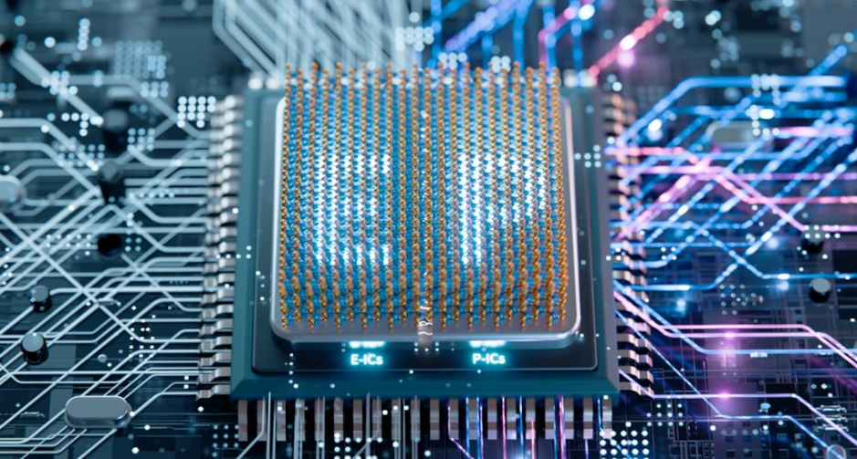
Photonic integrated circuits (Pics) are gradually becoming the core components of optical modules in 5G base stations and data centers. However, a chip of a centimeter integrates thousands of precise photonic components. Even minor differences in manufacturing and material defects can lead to substandard products. At this point, it is necessary to carry out targeted repairs on the defective chips. The technological advancements in laser repair have provided significant support for the production, manufacturing and subsequent improvement of optical chips.
I.
Opportunities and Challenges of Photonic Integrated Circuits
1.The Definition and Composition of Photonic Integrated Circuits
Photonic Integrated circuits (PIC), distinct from traditional electronic integrated circuits (IC) which integrate various electronic components such as transistors, capacitors and resistors, are compact integrated devices that integrate multiple photonic components and functions on a single chip. Optical or optoelectronic devices in PIC include lasers, electro-optic modulators, photodetectors, optical attenuators, optical multiplexers/demultiplexers, and optical amplifiers.
These devices are connected through optical waveguides to form photonic circuits, enabling the generation, transmission, detection and processing of optical signals. The information in photonic integrated circuits is created, modulated and measured in the form of optical signals.
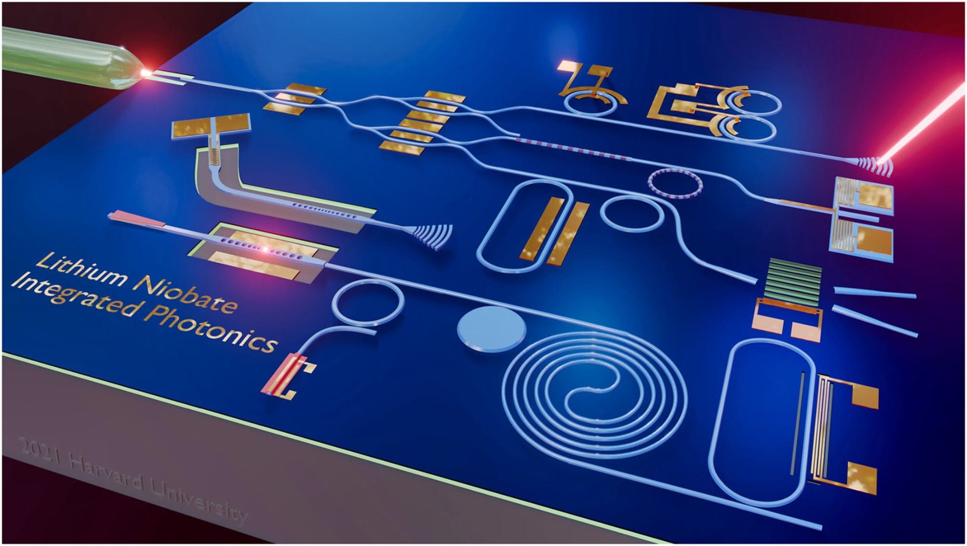
(Note: Image from online resources)
2.Applications of PIC
Photonic integrated circuits (PIC) have gradually developed into a mature and powerful technology in recent years. As the core of the next-generation information technology, they are replacing traditional electronic modes with optical signals to achieve higher speed and lower power consumption data transmission and processing, and are widely used in computing, communication, medical care, autonomous driving and other fields.
The application of optical chips include but are not limited to the following aspects: data centers, AI computing power, 5G/6G communication, autonomous driving, biomedicine and quantum computing, etc.
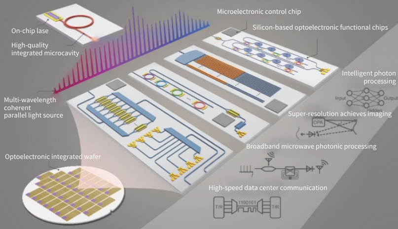
(Note: Image from online resources)
3.Problems Faced by PIC
In the design and manufacture of optical chips, the selection of waveguides - the core path for optical signal transmission, is closely related to specific application scenarios and the functional requirements of the chips. Optical chips in different applications have significantly different requirements for the optical performance and physical properties of waveguide materials. Therefore, materials with their own advantages are selected: silicon, lithium niobate, silicon dioxide, III-V semiconductors represented by indium phosphide and gallium arsenide, silicon nitride, and various polymers, etc., are all common waveguide materials.
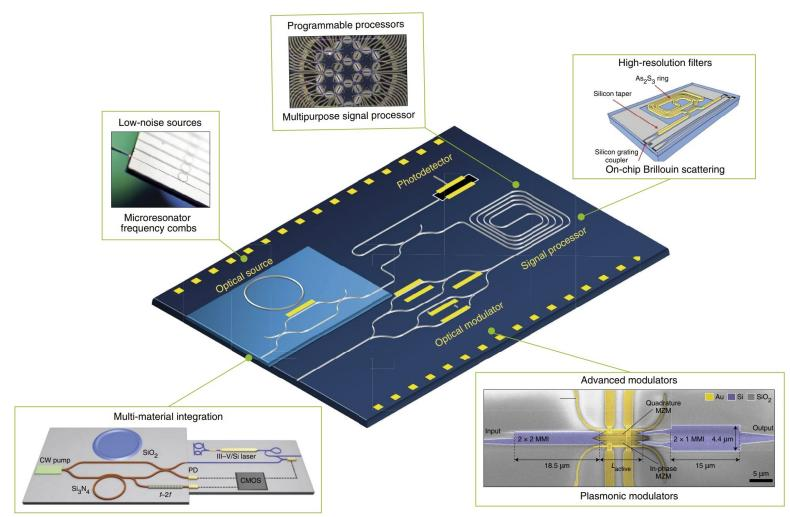
(Note: Image from online resources)
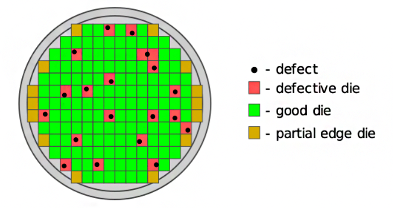
However, as the waveguide size of optical chips enters the sub-micron level - equivalent to one-thousandth of the diameter of a human hair or even smaller - this extremely small scale makes them highly sensitive to minute deviations in the manufacturing process. Specifically, whether it is tolerance fluctuations in the manufacturing process (such as slight deviations in etching accuracy), stress accumulation between different material film layers, or microscopic defects inherent in the material itself (such as lattice misalignment, impurity particles), even deviations at the micrometer or even nanometer level may have a significant impact on the optical guiding performance of the waveguide.
(Note: Image from online resources)
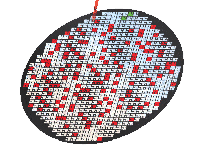
This high sensitivity directly brings about production challenges: on the one hand, it leads to the emergence of a large number of defective products whose performance does not meet the design standards; On the other hand, the performance of chips at different positions on the same wafer can also show significant differences - some have low signal transmission loss and fast response speed, while others have excessive loss and slow response, greatly reducing consistency. Ultimately, this will lead to an expansion of the performance fluctuation range of optical chips and a relatively low production yield. The insufficient yield will further increase the manufacturing cost per unit chip, which to a certain extent restricts the large-scale application of optical chips.
(Note: Image from online resources)
II.
Laser Repair of PIC
(Note: Image from online resources)
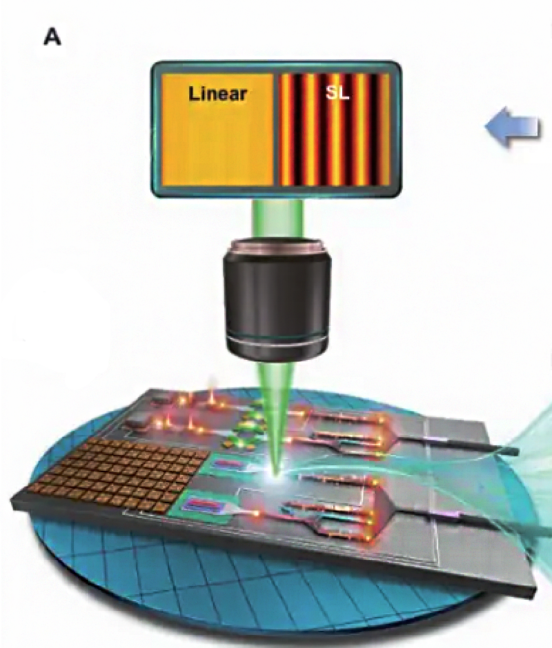
After the optical chip manufacturing is completed, it is usually necessary to correct the errors generated during the production process. The core idea is to achieve this by changing the refractive index of the waveguide or cladding material. Among the most commonly used repair methods at present, the method of regulating by the thermal light effect is relatively common. However, this method has obvious shortcomings: on the one hand, it will significantly increase the complexity of the repair system, and at the same time, it will increase the repair power consumption of the optical chip; On the other hand, its control range is extremely limited and can only be applied to specific optical waveguide positions with heating structures. This not only directly affects the cost-effectiveness of the optical chip system, leading to an increase in equipment investment and operating costs, but also restricts the accuracy of chip repair, making it difficult to meet the repair requirements of high-precision optical chips. Therefore, exploring a more efficient chip repair technology has become an urgent need for the industry.
(Note: Image from online resources)
Laser repair technology has unique performance advantages. Its ultra-short pulse duration, ultra-high peak power and sub-micron-level processing accuracy enable it to complete non-contact processing, modification and post-processing operations on the surface or inside of various materials such as metals, semiconductors and transparent media.
III.
CoreMorrow Piezo Nanotechnology: The "Golden Partner" for Laser Repair
The laser repair configuration for optical chips includes a test light source, a nano-scale multi-axis linkage displacement stage for placing the optical chip, and a receiving device. The multi-axis linkage displacement stage is fine-tuned to determine the positions of the structures in the optical chip that need to be corrected. The objective lens that can move up and down ensures the position and size of the focus point.
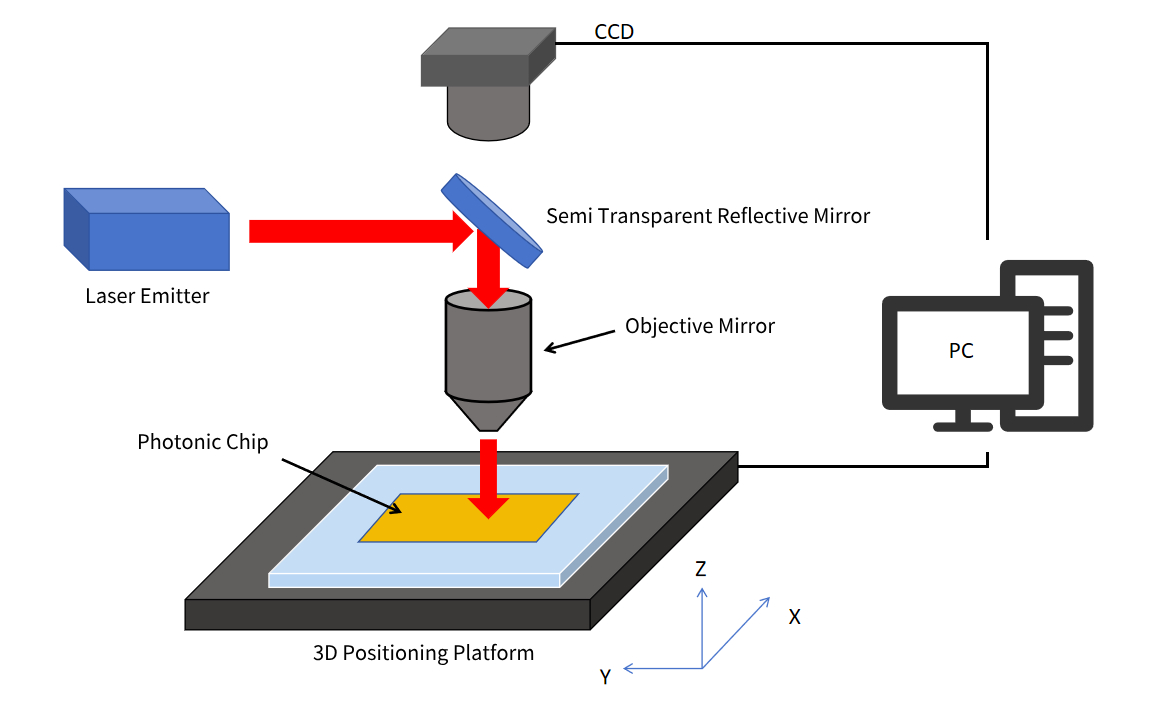
(Structure diagram)
Nanometer Positioning Accuracy: The width of photonic waveguides is usually at the sub-micron level. Repairing the light spot requires precise focusing to the micron or even nanometer level, which is difficult for traditional positioning systems to handle.
Millisecond Response:Laser repair requires dynamic path correction based on real-time optical feedback, which demands an extremely fast response speed of the positioning system.
Ultra-high Stability: The integrated structural design offers high rigidity and high load capacity, ensuring stability and reliability during the repair process.
Multi-axis Cooperative Control: It can simultaneously perform movements in multiple axes, achieving precise execution of complex repair paths.
CoreMorrow Piezoelectric Nanotechnology
Core Advantage
CoreMorrow Piezo Nanopositioning Stage
P65 piezo nanopositioning stage is drived by piezo actuators, combined with flexible hinge mechanism to realize XYZ motion. It is equipped with high-performance piezo actuators and amplified-drive mechanism to ensure XY200μm, Z50μm displacement. Open/closed loop versions available, vacuum and larger stroke version customizable. The closed-loop positioning accuracy can be up to XY0.017%F.S. and Z0.006%F.S., which is very suitable for high-precision positioning applications.
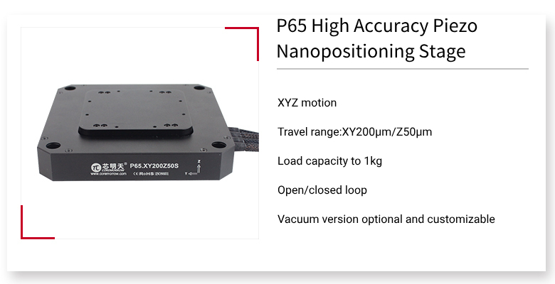
Typical Model
|
Model |
P65.XY200Z50S |
|---|---|
|
Active axes |
X、Y、Z |
|
Drive control |
8 driving channels, 8 sensing channels |
|
Travel range(0~120V) |
XY160μm/Z40μm |
|
Max.travel range(0~150V) |
XY200μm/Z50μm |
|
Sensor |
SGS |
|
Resolution |
XY3nm/Z2nm |
|
Closed-loop linearity |
XY0.015%F.S./Z0.007%F.S. |
|
Closed-loop Repeatability |
XY0.017%F.S./Z0.006%F.S. |
|
Pitch/yaw/roll |
<10μrad |
|
Unloaded resonant frequency |
X260Hz/Y220Hz/Z280Hz |
|
Rosonant frequency@500g |
150Hz |
|
Closed/open-loop unloaded step time |
100ms@500g |
|
Load capacity |
1kg |
|
El. capacitance |
XY13.6μF/Z3.2μF |
|
Material |
Steel, Aluminum |
|
Mass |
1.24kg |
CoreMorrow 6-Axis Motion Piezo Stage
H64 ultra-high resolution piezo nano-positioning stage uses piezo ceramics as the driving source and combines a flexible hinge mechanism to achieve 6 axes precise motion of XYZ, θx, θy and θz. It adops amplification mechanism drive. Open/closed-loop versions are available for your option. The closed-loop positioning accuracy can be up to 0.1%F.S., making it highly suitable for high-precision positioning applications.
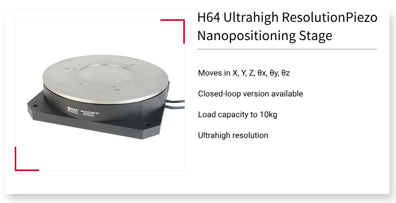
Typical Model
|
Model |
H64.XYZTR0S |
|---|---|
|
Active axis |
X、Y、Z、θx、θy、θz |
|
Drive/control |
6 driving channels, 6 sensing channels |
|
XYZ travel range(0~120V) |
XY14.4μm/Z30μm |
|
XYZ Max.travel range(0~150V) |
XY18μm/Z37.5μm |
|
θxθyθz Max.travel range(0~120V) |
θxθy0.32mrad(≈66”)/θz1.3mrad(≈268”) |
|
θxθyθz Max.travel range(0~150V) |
θxθy0.4mrad(≈83”)/θz1.6mrad(≈330”) |
|
Sensor |
SGS |
|
Closed-loop XYZ resolution |
XY0.6nm/Z1.25nm |
|
Closed-loop θxθyθz resolution |
θxθy13nrad/θz50nrad(<0.01”) |
|
Closed-loop linearity |
XYZ 0.02%F.S./Θxθyθz 0.1%F.S. |
|
Closed-loop repeatability |
XYZ 0.06%F.S./Θxθyθz 0.1%F.S. |
|
El. capacitance |
XY6.8μF/θxθyZ14.2μF/θz62.5μF |
|
Load capacity |
10kg |
|
Unloaded resonant frequency |
>150Hz |
|
Resonant frequency@10kg |
>100Hz |
|
Closed/open-loop step time |
60ms |
|
Mass |
9.5kg(Not including cable) |
|
Material |
Steel, Aluminum |
CoreMorrow Piezo Objective Scanner
P76 is a high-load Z-axis motionpiezo objective scanner, specially designed for objective lens focusing microscopy. It features a large load capacity up to 900g, Z-axis linear motion range up to 200μm, adopting flexible hinge mechanism, no friction, good linearity, high closed-loop positioning accuracy. The detachable threaded adapter design is compatible with various models of microscopes.
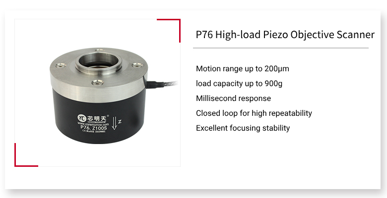
Typical Model
|
Model |
P76.Z100S |
|---|---|
|
Active axes |
Z |
|
Drive control |
1 driving channel, 1 sensing channel |
|
Travel range(0~120V) |
80μm |
|
Max.travel range(0~150V) |
100μm |
|
Sensor |
SGS |
|
Resolution |
2nm |
|
Closed-loop linearity |
0.03%F.S. |
|
Closed-loop repeatability |
0.02%F.S. |
|
Push/Pull force |
70N |
|
Stiffness |
0.8N/μm |
|
Unloaded resonant frequency |
800Hz |
|
Closed-loop working frequency(-3dB) |
160Hz(Unloaded) |
|
Closed/open-loop unloaded step time |
5ms |
|
Load capacity |
0.5kg |
|
El. capacitance |
7.2μF |
|
Material |
Steel, Aluminum |
|
Mass |
500g |
Note: The above parameters were measured using the E00/E01 controller. The maximum driving voltage can be within the range of -20V to 150V. For highly reliable long-term use, it is recommended that the driving voltage be between 0 and 120V.
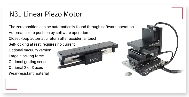
CoreMorrow Linear Piezo Motor
N31 linear piezoelectric motor adopts stick-slip principle, and piezo step direct drive. The linear motion range can be 6, 10, 25, 50 or 100mm, and the resolution can reach nanometer level. Closed-loop servo sensors (grating sensor) for high positioning accuracy and motion platform are available.
Typical Model
|
Model |
N31.100E |
|---|---|
|
Active axes |
X |
|
Integrated sensor |
Grating sensor |
|
Travel range |
100mm/±50mm |
|
Max. speed |
5mm/s |
|
Closed-loop resolution |
<50nm |
|
Linearity |
2μm |
|
Repeatability |
2μm |
|
Push/pull force(Active) |
30N |
|
Holding force(Passive) |
40N |
|
Max. Load (horizontal direction) |
5Kg |
|
Working temperature |
0~50℃ |
For further details, please call +86-451-86268790, or add WeChat ID: 17051647888.
Sweep, get the latest information on core tomorrow
Address:1F, Building I2, No.191 Xuefu Road, Nangang District, Harbin, China
Tel:0451-86268790
Piezo · Nano · Motion
