
How Crucial is Piezo Nano-positioning Technology in Probe Stage Applications
In the manufacturing process of semiconductor chips, probes can be used to test the performance of the chips. In the laboratory for new material research and development, the nanoscale contact between the probe and the sample surface unveils the electrical and optical properties of the material. In the biological research laboratory, probes are penetrating cells with extremely rapid and subtle movements. Behind all these precise operations lies a core device - the probe stage.
I
Probe Stage
A Testing Stage for the Microscopic World
Probe stage, as key equipment for modern micro-nano testing and manipulation, are widely used in semiconductor inspection, material research, biomedicine and other fields. It is like an operating table in the microscopic world, enabling researchers to precisely manipulate and measure nanomaterials, cells, and even individual molecules.
In simple terms, the core task of a probe stage is to achieve precise alignment and stable contact between the probe and the sample at the nanometer to micrometer scale, and to cooperate with testing instruments to complete the detection of force, electricity, light and other properties. Whether it is the yield detection of chips in the semiconductor industry, the characteristic analysis of new materials, or the parameter calibration of optoelectronic devices, the probe stage is an indispensable connecting bridge. It builds a channel between macroscopic testing equipment and microscopic samples, and its accuracy directly determines the reliability of the test data.
The core principle of the probe stage is to drive the probe or sample to move in multiple free dimensions and adjust the angle through precise mechanical structure and control technology, ensuring that the probe can accurately land on the test point of the sample. At the same time, it is necessary to maintain a stable contact force to avoid crushing the sample or poor contact.
(Note: Image from online resources)
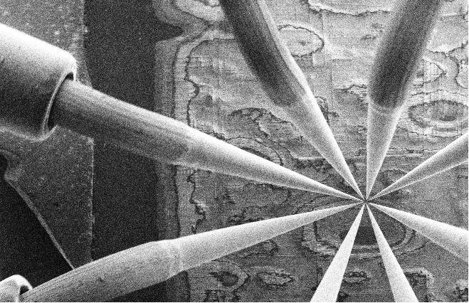
Nanoprobe
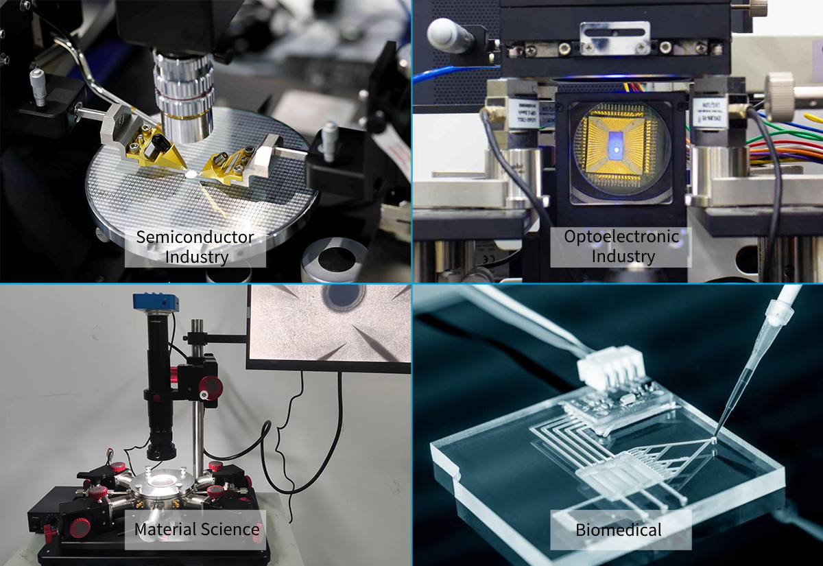
The Main Application Industries and Scenarios of Probe Stage
1.Semiconductor Industry: Electrical performance testing of integrated circuits, wafer testing, and post-packaging testing.
2.Optoelectronic industry: Test the performance of optoelectronic components such as leds, photodetectors and lasers.
3.Material Science: Characterizing the microscopic morphology of material surfaces, such as surface defects, grain size, etc. Research and test the electrical, magnetic, optical and other properties of materials at different temperatures, as well as the stability and reliability of the materials.
4. Biomedical: Research on the biocompatibility of biomaterial surfaces; High-resolution imaging, analysis of biomolecules, cells and tissues, as well as the development of biosensors, etc.
(Note: Image from online resources)
II
Why has Piezoelectric Nanotechnology
Gradually Become a Core Demand for Probe Stage?
From the perspective of the application scenarios of probe stage, whether it is chip inspection in the semiconductor industry or cell experiments in the field of biological research, these high-precision fields essentially rely on the extreme accuracy of the positioning and control technology of probe stations. When the operational accuracy requirements reach the nanometer level or even the sub-nanometer level, the traditional mechanical drive method has long been unable to meet the demands. The possible mechanical clearance may lead to errors, the slow response speed cannot adapt to high-frequency testing, and insufficient stability will affect data repeatability.
At this point, piezoelectric nano-positioning and control technology becomes the key to breaking the deadlock: based on the piezoelectric effect, through the inverse piezoelectric effect of piezoelectric materials, displacement control, angle adjustment and dynamic response at the nanometer or even sub-nanometer level can be achieved, perfectly meeting the core requirements of the probe station for "high precision, high stability and fast response".
 The Core Advantages of Piezoelectric Nanotechnology
· Nanometer-level resolution: Motion accuracy of nanometers and below is required
· Ultra-high stability: Avoid the influence of vibration on precise operations
· Fast response: Millisecond-level response speed to adapt to dynamic testing
· Vacuum compatibility: Adapted to the high vacuum environment of microscopic equipment such as SEM
· Multi-axis collaboration: It can achieve multi-dimensional and complex angle control
III
CoreMorrow
Piezoelectric Nanoprobe Stage has shown its Prowess
1.15-axis Piezo Nanoprobe Stage: A Collaborative Process of High-precision Piezoelectric Technology
CoreMorrrow piezoelectric nano-probe stage is composed of a piezo nano-positioning stage, a piezo motor, a piezo objective scanner and structural components. The piezo nano-positioning stage, as a sample carrying platform, can achieve 2-axis high-precision tip/tilt. The probes, respectively controlled by four piezo motion stages, which can achieve nanometer-level precision movement in XYZ. The piezo objective scanner precisely controls the objective lens to perform nanoscale focusing adjustment in Z to achieve high-resolution microscopic observation.
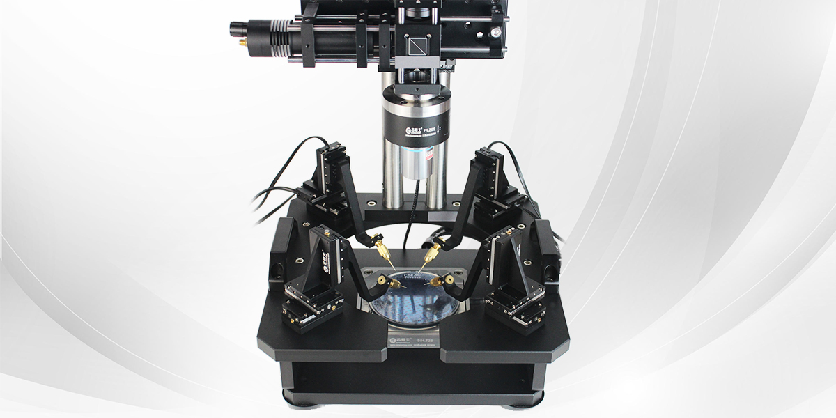
1) Sample Carrying Platform
The piezo nano-positioning stage is a piezo platform that can achieve single-axis or even multi-axis precise motion. Its motion range can be down to millimeter level. It features small size, no friction, and fast response speed. Equipped with high-precision sensors, it can achieve nanometer-level resolution and positioning accuracy. The design features of high rigidity and zero gap ensure the stability and repeatability of the system during operation, making it a reliable platform for carrying samples.
2)Probe Stage
The piezo motor uses piezo ceramics as the driving motor. With a special mechanical structure design, it converts the linear micro-displacement generated by the piezo ceramics into macroscopic linear (or angular) motion in the mechanical plane, with a travel range of up to tens of millimeters (or 360°). The nanometer-level repeatability enables it to achieve high-precision positioning of probes. In response to the demand for controlling the force exerted by the probe on the sample, CoreMorrow piezo motor offers nanoscale motion control and precise force output, providing accurate positioning and navigation for the probe's movement.
3)Microscopic Focusing
When operating on microscopic samples such as biological cells, it is necessary to maintain both the clarity of sample observation and the accuracy of probe operation simultaneously. CoreMorrow piezo objective scanner is specially designed for objective lens focusing microscopy. It adopts a flexible hinge without hysteresis and a parallel guiding mechanism design, with a small objective lens compensation amount and ultra-high focusing stability. The objective scanner is installed in the microscopic detection/measurement or observation device, which can drive the objective lens to focus and improve accuracy. It can be used in conjunction with various high-resolution microscopes and can achieve nanoscale coordinated positioning of samples and optical systems.
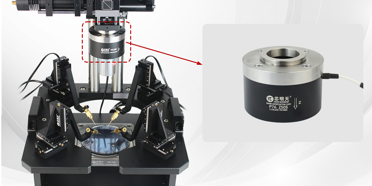
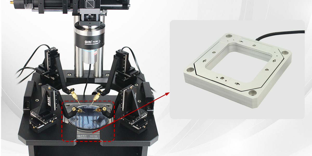
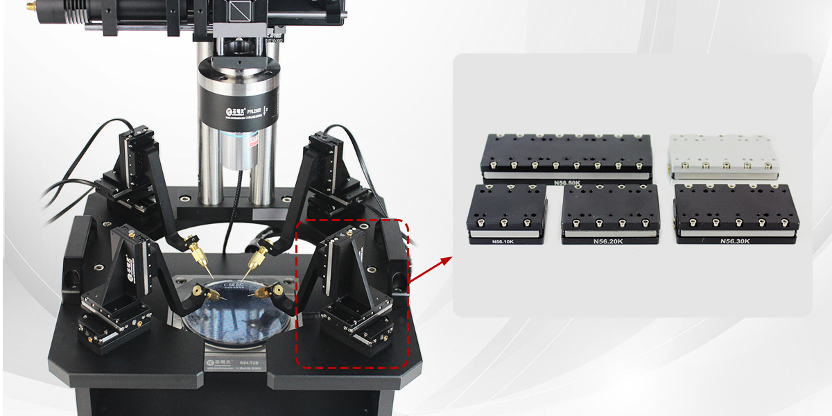
The probe stage shown in the figure integrates multiple piezo products of CoreMorrow. Its core configuration includes: the S54 θx,θy tip/tilt stage, whose parameters can be customized according to actual needs. The N56 series linear motor stage features a wide range of selectable strokes, with the maximum stroke of 50mm. Piezo objective scanner, multiple travel options available, with a maximum resolution of up to 2.5nm.
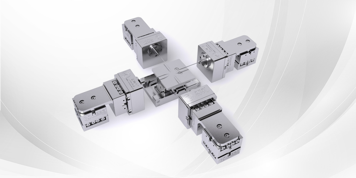
2.19-axis Piezo Nanoprobe Stage: The Perfect Integration of Micro-nano Operations
CoreMorrow piezo nanoprobe stage integrates a piezo nanopositioning stage and four nanoprobe modules based on a piezo motor driven stage. It can be used in conjunction with scanning electron microscopes (SEM), transmission electron microscopes (TEM), and other electron microscopes for nanoscale operations. The sample platform at the center can perform XYZ motion, and the four sets of nanoprobe modules can perform XYZ linear and R-axis rotation. The dimensions, active axis, stroke and speed of the nano-probe station can be customized.
|
Piezo Nanoprobe Stage |
|
|
Nanoprobe Stage |
|
|
Active axis |
XYZ |
|
Resolution in Z |
≤2nm |
|
Travel range in Z |
≥20μm |
|
Travel range in XY |
≥20mm |
|
Travel speed in XY |
≥30mm/s |
|
Nanoprobe module |
|
|
Active axis |
XYZ linear motion and R rotaion |
|
Positioning resolution in XYZ |
≤100nm |
|
Travel range in XY |
≥5mm |
|
Travel range in Z |
≥0.5mm |
|
Travel range in R |
180° |
|
Scanning resolution |
≤2nm |
|
Operating Condition |
|
|
Scanning resolution |
10^-4Pa |
|
Operating temperature |
-45℃~100℃ |
|
Custom Parameters |
Parameters such as dimensions, interfaces, active axes, strokes, and speeds can be customized |
For further details, please call +86-451-86268790, or add WeChat ID: 17051647888.
Sweep, get the latest information on core tomorrow
Address:1F, Building I2, No.191 Xuefu Road, Nangang District, Harbin, China
Tel:0451-86268790
Piezo · Nano · Motion
