
How Can Piezo Nanotech Boost Adhesive Coating Precision & Equipment Development
01
Piezoelectric Nanotechnology has Shown its Prowess in Adhesive Coating and Developing Equipment
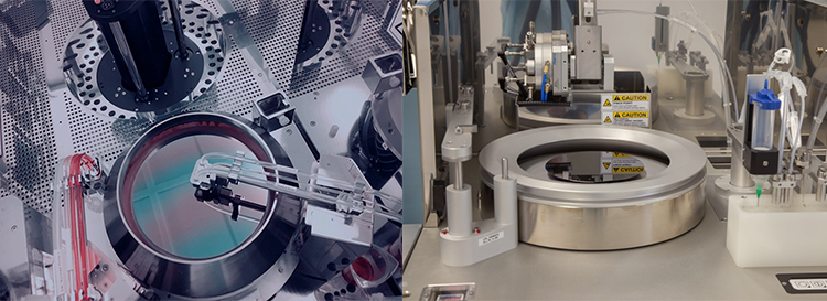
In the photolithography process of semiconductor manufacturing, coating and developing equipment and photolithography machines need to work in coordination to jointly achieve precise photolithography processes. Before the exposure process, the photoresist will be evenly coated on the surface of the wafer. After the exposure is completed, the developing equipment processes the wafer and develops the photolithography pattern formed by the exposure. The entire process has extremely high requirements for equipment performance. It is necessary to complete the response within milliseconds while ensuring nanomet-level operational accuracy. Only in this way can the accuracy and stability of the photolithography process be guaranteed, and the manufacturing quality of semiconductor devices be ensured.
(Note: Image from online resources)
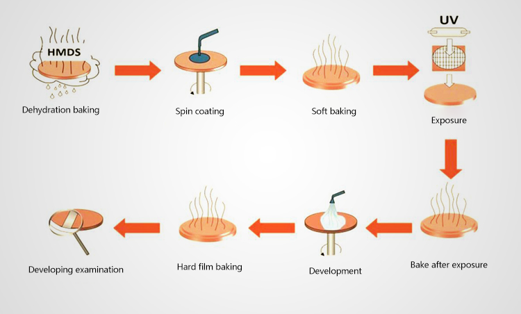
The Photoresist Application Process:
The photoresist is evenly coated on the wafer surface through spin coating or spray coating. There are static spin coating and dynamic spin coating. Static spin coating is a process where glue is dropped while the wafer is stationary. The turntable drives the wafer to rotate, completing the process of glue ejection and solvent evaporation. Dynamic spin coating is a process in which the wafer undergoes low-speed rotation while dripping glue, and then accelerates the rotation to complete the glue ejection and solvent evaporation. The photoresist spraying is to spray the photoresist onto the wafer surface in the form of "glue mist" through the glue nozzles that move back and forth along a specific trajectory by the glue spraying equipment.
(Note: Image from online resources)
The Developing Process:
After exposure, the wafer is treated with a developing solution, which is usually an acidic or alkaline solution that can dissolve the photoresist or change its physical properties, making it easier to remove. During the development process, the wafer is immersed in the developing solution for a period of time. The developing solution undergoes a chemical reaction with the photoresist, dissolving or retaining the unexposed photoresist, thereby forming a pattern corresponding to the mask.
(Note: Image from online resources)
The key to applying adhesive lies in controlling the thickness and uniformity of the adhesive film, and it is necessary to precisely control parameters such as the rotational speed and the landing point of the sprayed adhesive.
During the development process, the positioning accuracy of the wafer and the uniformity of the developer spray directly affect the line width accuracy and edge roughness of the pattern.
Ultra-Precision Control:
The rotational speed stability of the gluing machine needs to be controlled within a very small range to ensure the uniformity of the photoresist thickness.
Temperature Control:
The temperature control of the baking chamber must precisely meet the strict standard of an error not exceeding 0.1 degrees.
Wafer Processing Safety:
Wafers should be kept stable during processing and transportation between equipment to avoid damage.
Chemical Stability:
The key components in the equipment need to withstand the long-term corrosion of various chemical reagents.
02
Piezoelectric Nanotechnology has Shown its Prowess in Adhesive Coating and Developing Equipment
The Advantages of Piezoelectric Nanotechnology:
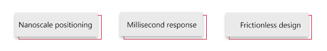
1.Nanometer-Level Positioning Resolution:Through the inverse piezoelectric effect of piezoelectric ceramics, nanometer-level displacement control is achieved, which can perfectly match the nanometer-level requirements for the thickness of the adhesive film during the application process.
2.Millisecond-level Dynamic Response:Piezoelectric drive has almost no mechanical transmission gap, and the response time can be up to millisecond level. It can be combined with a closed-loop feedback system to follow the high-speed rotation of the wafer in real time or quickly locate the spray position, avoiding pattern offset caused by motion lag.
3.Frictionless and Low-Vibration Design:The piezoelectric nano-platform adopts a frictionless flexible hinge guiding mechanism inside, resulting in minimal mechanical wear. The vibration amplitude during operation is controlled within the nanometer range, eliminating the tremor error that may be caused by traditional mechanical drive, and is suitable for the strict requirements of wafer stability during development.
03
CoreMorrow Piezoelectric Nanotechnology: Infusing "Precision Soul" into Adhesive“ Coating and Developing Equipment”
CoreMorrow Piezoelectric Nanopositioning Stage
The piezoelectric nanopositioning stage is a piezoelectric platform that uses piezoelectric ceramics as the driving source and combines a flexible hinge mechanism to achieve precise motion in the X, Z, XY, XZ, XYZ and 6 axes. The driving forms include piezoelectric ceramic direct drive mechanism and amplification mechanism. The motion range can be up to millimeter level, featuring small size, no friction, and fast response speed. Equipped with high-precision sensors, it can achieve nanometer resolution and positioning accuracy. CoreMorrow piezoelectric nanopositioning stage plays a crucial role in the field of precise positioning.
H64 6-Axis Piezoelectric Nanopositioning Stage
H64 ultra-high resolution piezoelectric nanopositioning stage is a piezoelectric platform that uses piezoelectric ceramics as the driving source and combines a flexible hinge mechanism to achieve 6-axis precise motion along X, Y, Z, θx, θy, and θz. It adopts amplification mechanism drive. Open/closed-loop versions are available. The closed-loop positioning accuracy can be up to 0.1%F.S., making it highly suitable for high-precision positioning applications.
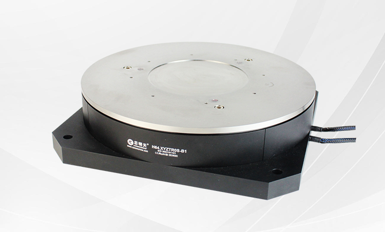
Characteristics
▲6-axis motion of X, Y, Z, θx, θy, and θz
▲ Optional closed-loop feedback sensor
▲Load capacity up to 10kg
▲Ultra-high resolution
Technical Data
|
Model |
H64.XYZTR0S |
|
Active axis |
X、Y、Z、θx、θy、θz |
|
Drive control |
6 driving channels, 6 sensing channels |
|
XYZ travel range(0~120V) |
XY14.4μm/Z30μm |
|
XYZ Max.travel range(0~150V) |
XY18μm/Z37.5μm |
|
θxθyθz travel range(0~120V) |
θxθy0.32mrad(≈66")/θz1.3mrad(≈268") |
|
θxθyθz Max.travel range(0~150V) |
θxθy0.4mrad(≈83")/θz1.6mrad(≈330") |
|
Sensor |
SGS |
|
Closed-loop linear resolution |
XY0.6nm/Z1.25nm |
|
Closed-loop angular resolution |
θxθy13nrad/θz50nrad(<0.01") |
|
Closed-loop linearity |
Linear0.02%F.S./Rotation0.1%F.S. |
|
Closed-loop repeatability |
Linear0.06%F.S./Rotation0.1%F.S. |
|
El. capacitance |
XY6.8μF/θxθyZ14.2μF/θz62.5μF |
|
Load capacity |
10kg |
|
Unloaded resonant frequency |
>150Hz |
|
Loaded resonant frequency@10kg |
>100Hz |
|
Closed-loop step time |
60ms |
|
Mass |
9.5kg (exclude cable) |
|
Material |
Steel, Al |
H64A.XYZTR2S/K-C 6-Axis Motion Piezo Stage
H64A.XYZTR2S/K-C is a piezo nanopositioning platform that can generate ultra precision motion in 6 axes, suitable for positioning and attitude adjustment. It adopts a parallel mechanism design internally, which can achieve better dynamic performance. It is equipped with high-performance piezos, which can achieve linear displacement of ±9μm in X, ±9.5μm in Y, 155μm in Z and deflection angle of ±1.1mrad in θx,θy, ±1mrad in θz. The closed-loop version of the full bridge design avoids temperature drift significantly and ensures nanometer positioning accuracy.。
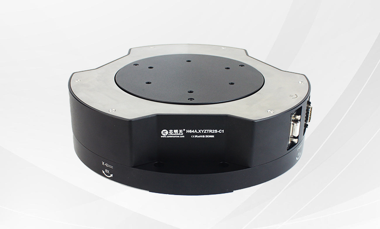
Characteristics
▲Moves in X, Y, Z, θx, θy, θz
▲Linear stroke to X±9/Y±9.5/Z155μm
▲Angular stroke to θxθy±1.1/θz±1mrad
▲Closed-loop version for high positioning accuracy
▲Parallel mechanism, better dynamics
▲Load capacity to 12kg
Technical Data
|
Model |
H64A.XYZTR2S-C |
|
Active axis |
X、Y、Z、θx、θy、θz |
|
Drive control |
6 driving channels, 6 sensing channels |
|
XYZ travel range(0~120V) |
X±7μm/Y±7.5μm/Z125μm |
|
XYZ Max.travel range(0~150V) |
X±9μm/Y±9.5μm/Z155μm |
|
θxθyθz travel range(0~120V) |
θxθy±0.9mrad(≈±186")/θz±0.8mrad(≈±165") |
|
θxθyθz Max.travel range(0~150V) |
θxθy±1.1mrad(≈±227")/θz±1mrad(≈±206") |
|
Sensor |
SGS |
|
Closed-loop linear resolution |
X0.56nm/Y0.61nm/Z5nm |
|
Closed-loop angular resolution |
θxθy0.08μrad/θz0.07μrad(≈0.015") |
|
Closed-loop linearity |
Linear:0.05%F.S./Angular:0.02%F.S. |
|
Closed-loop repeatability |
0.02%F.S. |
|
Loaded resonant frequency@10kg |
>109Hz |
|
Load capacity |
12kg |
|
El. capacitance |
XY7.2μF/θxθyZ21.6μF/θz50μF |
|
Closed-loop step time |
40ms@1Hz,1/100stroke |
|
Material |
Steel, Al |
|
Mass |
6.45(exclude cable) |
|
Connector |
DB15 male ×1+DB15 female ×1 |
Note: The above parameters were measured with E00.D6K04 piezo controller. The limit of the driving voltage can be within -20V to 150V. For highly reliable long-term use, it is recommended that the driving voltage between 0 and 120V.
CoreMorrow Piezoelectric Ceramic Actuator
In the adhesive coating and developing process, piezoelectric ceramic actuators can precisely control: the opening and closing accuracy of valves, the amount of adhesive sprayed, and the fine-tuning of wafer transmission, etc. CoreMorrow piezoelectric ceramic actuator features an extremely fast response time of microseconds, a frequency of up to several thousand Hertz, and a displacement of micrometers, ensuring the process stability of the equipment during high-speed operation.
Cylindrical Piezo Actuator
The cylindrical piezo actuator is to package the piezo stack into a steel casing and apply preload to the piezo stacks. The high internal mechanical preload makes the piezo stacks suitable for high-load and high-dynamic applications. It can output the displacement and output force generated by the piezo stacks, and can withstand a certain tensile force.
√Direct Drive Structure:
The ceramic actuator adopts a piezo ceramic direct drive structure, featuring high blocking force and fast response speed. It can be optionally equipped with sensors for closed-loop feedback. The top and bottom of the piezo ceramic actuator are fixed respectively by threads. The fixing method can be customized, such as external thread, internal thread, Spherical and plane, etc.
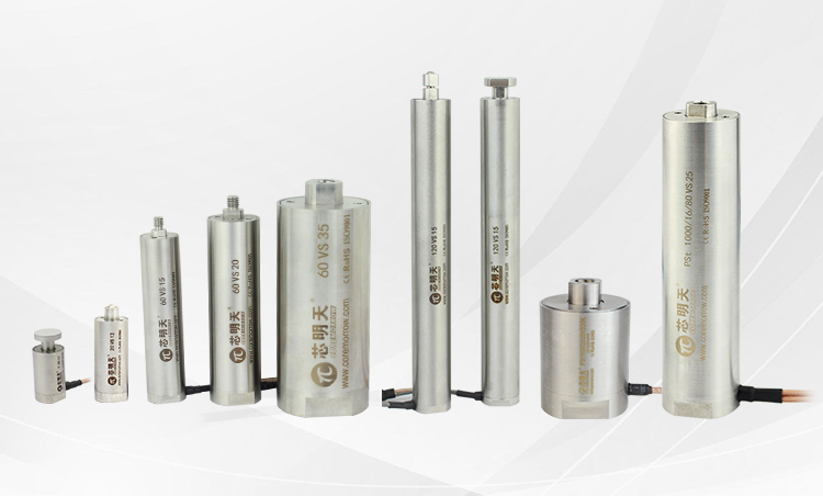
Characteristics
▲Nanoscale resolution
▲Bear a certain tensile force
▲High closed-loop accuracy
▲Travel to 190μm
▲Blocking force to 25000N
Technical Data
|
Model |
Cylindrical Piezo Actuator |
|
Displacement |
8μm~200μm |
|
Stiffness |
5N/μm~4000N/μm |
|
Push//Pull force |
200/30N~50000/6000N |
|
El. capacitance |
0.17μF~6500μF |
|
Resonance Frequency |
3kHz~40kHz |
|
Length |
19mm~200mm |
Metal-sealed Preloaded Piezo Actuator
Metal-sealed preloaded piezo actuators have a fully sealed casing, achieving insulation from the atmospheric environment and being less affected by environmental humidity. They have a longer service life and higher performance, making them very suitable for various applications such as semiconductor device manufacturing equipment and optical communication equipment that require high reliability.
Characteristics
▲High reliability: Realization of MTTF=36,000 hours at 85°C and 100 V
▲Accurate nanometer positioning
▲Minimum mechanical abrasion
▲Operation temperature::−25℃ ~+85℃(H&S series)or -40~150℃ (T series)
▲Blocking force to 3600N 3600N
▲Driving Voltage:0~150V0~150V
▲Built-in pre-load mechanism and mounting attachments allowing for easier installation into equipment
Note: MTTF: Mean Time To Failures
Typical Model
H550C801WD1-A0LF is one of CoreMorrow preloaded piezo actuators. It has 55μm displacement and 800N force. The high-standard performance makes it very suitable for driving fluid flow control valves, meeting the high reliability and high precision requirements of fluid flow control valves for driving components. There are other models and custom specifications available for your option.

Technical Data
|
Model |
H550C801WD1-A0LF |
|
Displacement |
55±8μm |
|
Generated force |
800N |
|
Capacitance |
6.4μF |
|
Resonance Frequency |
18kHz |
|
Type |
Without flange |
|
Weight |
16g |
|
Working temperature |
-25~85℃ |
|
Length |
44.4±0.5mm |
For further details, please call +86-451-86268790, or add WeChat ID: 17051647888.
Sweep, get the latest information on core tomorrow
Address:1F, Building I2, No.191 Xuefu Road, Nangang District, Harbin, China
Tel:0451-86268790
Piezo · Nano · Motion
