
How CoreMorrow Piezo Nanotech Helps Etching Machines Reach Precision Ceiling
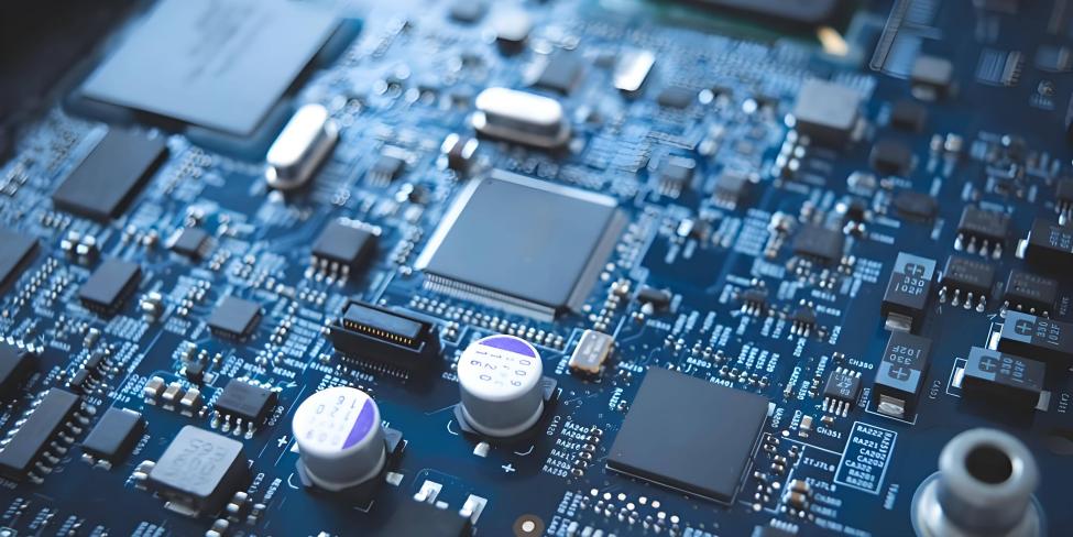
In the semiconductor manufacturing process, the birth of each nanoscale chip is underpinned by an extremely precise competition at the atomic level. In this "precision battle" of the microscopic world, the etching machine can be regarded as the best partner of the photolithography machine. The two work together to drive the precision process of chip manufacturing. Their performance and collaborative level not only lay the foundation for the precision of chip manufacturing, but also fundamentally determine the development direction and upper limit of the entire process accuracy.
(Note: Image from online resources)
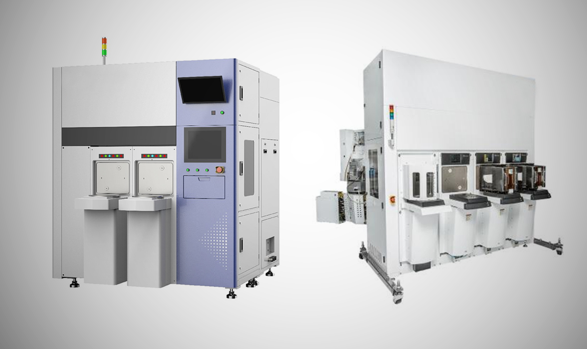
Etching technology is an indispensable part of the chip manufacturing process. Etching machines are used in semiconductor manufacturing for etching processes. Their core function is to selectively remove specific material layers on the surface of wafers, permanently transferring the photoresist patterns defined by the photolithography process to the actual material layers below (such as silicon, oxides, metals, etc.), and ultimately forming key structures such as transistors, interconnects, and grooves inside the chip.
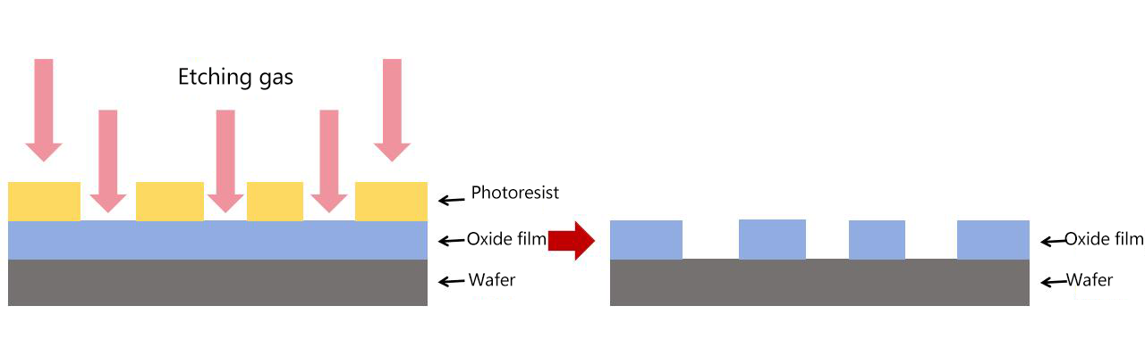
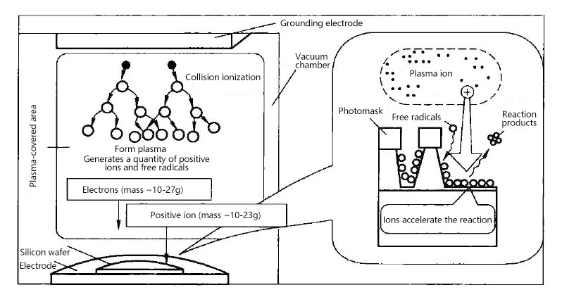
Etching equipment is mainly classified into wet etching and dry etching based on the differences in processes. Wet etching usually employs chemical solutions, while dry etching typically uses plasma or specific gases. At present, in pursuit of higher precision in semiconductor manufacturing, especially in advanced processes, dry etching is mostly adopted. The core principle of dry etching is as follows: a specific etching gas is introduced into the reaction chamber of the etching machine. The gas is ionized by a radio frequency power supply to form plasma, which then undergoes a chemical reaction with the target material on the wafer surface. The products generated by the reaction are removed, thereby precisely transferring the pattern on the photoresist to the material layer below.
(Note: Image from online resources)
In summary, etching machines, like photolithography machines, are key equipment for forming patterns on semiconductor chips, and their precision directly determines the integration and performance of the chips.
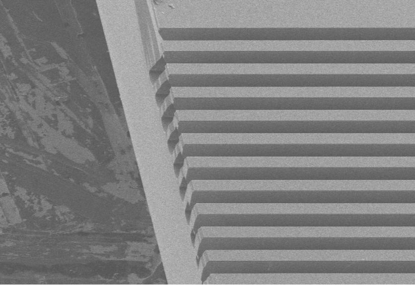
As chip manufacturing processes progress from 14nm to 3nm, 2nm, and even more advanced nodes in the future, the dimensional accuracy and shape control of etching are gradually approaching physical limits.
(Note: Image from online resources)
1. Nanoscale Size and Edge Roughness: The critical size of transistors has been reduced to a few nanometers, and the edge roughness of the etched pattern also needs to be controlled at the nanometer level; otherwise, it may cause current fluctuations and unstable performance of the device.
2. Etching Depth Control: The etching depth needs to be precise to nanometers. Excessive etching can damage the underlying material, while insufficient etching will result in incomplete pattern transfer. Both will reduce the yield of the chip.
3. Uniformity Control: When the wafer is too large, the distance between the edge and the center is relatively large. Even minor differences in plasma density, gas flow rate, and temperature distribution can lead to uneven etching rates. It is necessary to maintain nanoscale etching uniformity.
4.Positioning and Synchronization: The mechanical system of the etching machine needs to achieve sub-nanometer level motion accuracy and long-term stability. During the etching process, the wafer must be precisely aligned with the pattern defined by the photolithography.
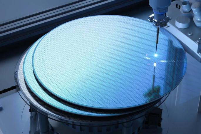
(Note: Image from online resources)
The core advantage of piezo nano-positioning technology lies in its low-energy consumption precision motion control with nanoscale resolution and millisecond-level response speed.
① Nanometer-level resolution: Achieve nanometer-level control of wafer displacement to meet the requirements of smaller steps.
② Millisecond-level response: Ultra-fast response speed, capable of achieving dynamic compensation dozens of times faster than traditional braking.
③Stability and Anti-Interference: Mechanical vibrations and temperature fluctuations generated during the operation of the etching machine may affect positioning accuracy. The integrated rigid structure design of piezoelectric nano products significantly reduces vibration transmission and is not affected by temperature, minimizing drift.
Core Technological Advantages
1. Nanoscale Displacement Adjustment of Wafers
The positioning accuracy of the wafer during the etching process directly affects the process effect. The piezo nano-positioning stage can perform multi-dimensional precise angle adjustment, featuring extremely high positioning accuracy and stability, with a fast response speed. It can ensure the ideal relative position between the wafer and the plasma flow, eliminating the etching deviation problem caused by offset.
(Note: Image from online resources)
2. Control of Etching Morphology
Facing the etching challenges of stereo circuits on chips, piezo ceramic actuators can assist RF electrodes in fine-tuning, real-time correcting the position of the plasma beam, optimizing the plasma distribution, achieving undamaged etching shapes and distortion-free line width, and meeting the precise etching requirements of key structures in chips. Meanwhile, the lifespan of high-performance piezoelectric actuators exceeds one billion reciprocating cycles, which can meet the long-term mass production demands of etching machines.
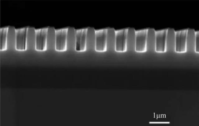
(Note: Image from online resources)
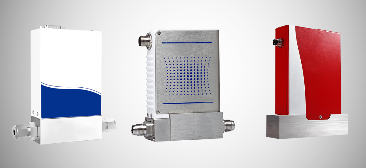
3.Microfluidic Control of Etching Gas
The flow rate of the etching gas needs to be precise to the error level of less than 0.1%, and the gas formula needs to be switched within milliseconds, such as from the etching medium layer to the etching metal layer, etc. This requires the adoption of high-precision mass flow controllers (MFC), and the response time of the internal valves of the MFC also needs to be controlled at the millisecond level. Moreover, the accuracy and stability should be minimized after long-term use.
(Note: Image from online resources)
CoreMorrow Piezo Nanopostioning Scanners
P15 is a fast, high-precision scanning and nanopositioning stage with very high straightness. It has multiple sizes of aperture which is ideal for transmitted-light applications such as near field scanning, confocal microscopy and mask positioning. P15 has 300μm displacement and its internal finite element analysis (FEA) optimized wire-cut flexural hinge structure. FEA gives it the design with the highest possible stiffness and minimizes linear and angular runout.
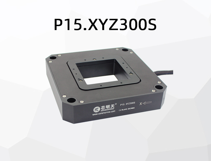
Characteristics
• 2 axes or 3 axes, travel to 300μm/axis
• Frictionless, high precision flexible guiding system
• Closed-loop sensor available
• High scanning flatness
• Multiple sizes of aperture available
• UHV version available
Technical Data
|
Model |
P15.XYZ300S |
|---|---|
|
Active axes |
X、Y、Z |
|
Drive control |
3 driving channels, 3 sensing channels |
|
Travel(0~120V) |
240μm/axis |
|
Max.Travel(0~150V) |
300μm/axis |
|
Sensor |
SGS |
|
Aperture |
66mm×66mm |
|
Closed loop resolution |
8nm |
|
Closed loop repeatability |
0.1%F.S. |
|
Push/pull force |
50N/10N |
|
Stiffness |
0.1N/μm |
|
Unloaded resonant frequency |
140Hz/170Hz/220Hz |
|
Closed/open-loop unloaded step time |
60ms |
|
Load capacity (Horizontal) |
0.5kg |
|
El. capacitance |
XY10.8μF/Z13.2μF |
|
Material |
Al |
|
Mass |
0.83kg |
Note: Custom ultra-low temperature version and UHV version available.
CoreMorrow 6-axis positioning system
H60 Piezo Hexapod is a piezo stage with 6-axis motion of θx, θy, θz, X, Y, and Z. 6-axis movement in space is realized by the coordinated expansion and contraction of six piezoelectric actuators. It has a compact structure and three specifications and models available. The closed-loop model has high positioning accuracy, which is suited for applications such as microelectronics precision machining, test, etc.
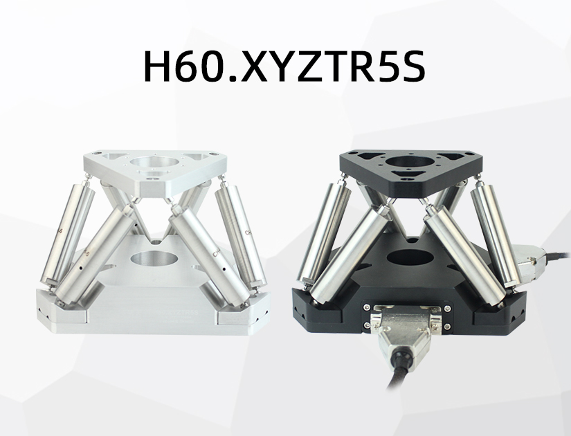
Characteristics
• Motion in X, Y, Z, θx, θy, θz
• Small coupling
• Closed-loop version for high accuracy
• No accumulation of error
Technical Data
|
Model |
H60.XYZTR5S |
|---|---|
|
Active axes |
X,Y,Z,θx,θy,θz |
|
Drive control |
6 driving channels, 6 sensing channels |
|
Linear travel in X, Y (0~120V)
|
±40µm |
|
Linear travel in Z (0~120V) |
±28µm |
|
Tilt angle in θx, θy(0~120V) |
±0.65mrad(≈±134") |
|
Tilt angle in θz(0~120V) |
±0.9mrad(≈±186") |
|
Sensor |
SGS |
|
Tilt resolution(θx, θy) |
0.4μrad |
|
Tilt resolution, θz |
0.5μrad |
|
Resolution in X, Y |
5nm |
|
Resolution in Z |
3nm |
|
Closed-loop repeatability |
0.1%F.S. |
|
Load capacity |
5kg |
|
Working temperture* |
-20~80°C |
|
Material |
Steel, Aluminum |
|
Mass |
1100g |
Note: Custom low temperature version and HV version available.
CoreMorrow Metal-sealed Preloaded Piezo Actuator
Metal-sealed preloaded piezo actuators have a fully sealed casing, achieving insulation from the atmospheric environment and being less affected by environmental humidity. They have a longer service life and higher performance, making them very suitable for various applications such as semiconductor device manufacturing equipment and optical communication equipment that require high reliability.
Characteristics
▲ High reliability: Realization of MTTF=36,000 hours at 85°C and 100 V
▲ Accurate nanometer positioning
▲ Minimum mechanical abrasion
▲ Operation temperature:−25℃ ~+85℃(H&S series)or -40~150℃ (T series)
▲ Blocking force to 3600N
▲ Driving Voltage:0~150V
▲ Built-in pre-load mechanism and mounting attachments allowing for easier installation into equipment
Note: MTTF: Mean Time To Failures
Typical Model
H550C801WD1-A0LF is one of CoreMorrow preloaded piezo actuators. It has 55μm displacement and 800N force. The high-standard performance makes it very suitable for driving fluid flow control valves, meeting the high reliability and high precision requirements of fluid flow control valves for driving components. There are other models and custom specifications available for your option.
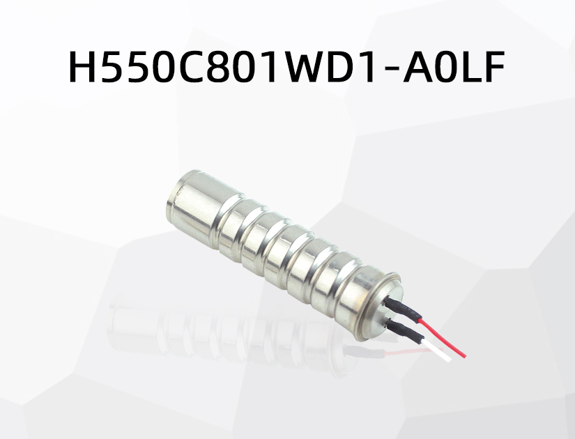
Technical Data
|
Model |
H550C801WD1-A0LF |
|---|---|
|
Displacement |
55±8μm |
|
Generated force |
800N |
|
Capacitance |
6.4μF |
|
Resonance Frequency |
18kHz |
|
Type |
Without flange |
|
Weight |
16g |
|
Working temperature |
-25~85℃ |
|
Length |
44.4±0.5mm |
For further details, please call +86-451-86268790, or add WeChat ID: 17051647888.
Sweep, get the latest information on core tomorrow
Address:1F, Building I2, No.191 Xuefu Road, Nangang District, Harbin, China
Tel:0451-86268790
Piezo · Nano · Motion
