
- Introduction
- Feedback
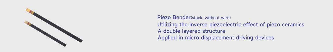
Piezo bender is a bending element that utilizes the inverse piezoelectric effect of piezo ceramics to generate lateral displacement under the driving force of an electric field. Structurally, it adopts a double layered structure, with two layers of piezo ceramic sheets arranged in the same polarization direction and tightly bonded to the middle electrode layer. Under the driving force of an alternating power source, it generates corresponding vibration amplitude and is applied in micro displacement driving devices.
Product Mix

The piezo benders consist of two piezo ceramic sheets and one metal sheet, arranged in the order of piezo ceramic sheets, metal sheets, and piezo sheets. The piezo benders have a non actuation region (no piezoelectric effect, no displacement) and an actuation region (with piezoelectric effect, displacement). The non actuation region can be used for fixation, but do not fix the metal electrode part to avoid short circuits or electrical connections. The piezo bender has three electrode points. The structure is shown in the following figure.
|
|

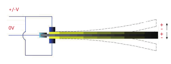
| Driving method 1(DC, bidirectional motion): | |

|
The wiring method is shown in the above figure.This driving method requires 2 channels of constant voltage (0V and positive voltage +V respectively) and 1 channel of variable voltage (range from 0 to+V). The voltage value of this +V must be within the voltage range specified in the parameter table and cannot be used under overvoltage, otherwise it will cause damage to the piezo ceramic.
For example: MTP60×20×0.8 piezo bending plate, its driving voltage upper limit is 150V. To achieve its upper limit of motion range, the controller requires three channels, one of which is 0V (output 0V constant voltage), one is +V (output 150V constant voltage), and the other is 0/+V (output 0~150V variable voltage). Within this voltage driving range, the upper limit of deformation displacement can be reached.
|
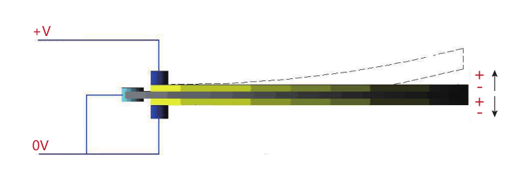
| Driving method2(AC, bidirectional movement): | |
|
The wiring method is shown in the above figure.该驱动方式需要1路交流电压+/-V,This driving method requires one AC voltage of+/- V, and the effective AC voltage of this series of piezo ceramic bending pieces must not exceed 50V (for sine wave voltage driving, the peak-peak voltage must not exceed 70V). Do not use under overvoltage, otherwise it will cause damage to the piezo ceramic. For example: MTP60×20×0.8 piezo bending plate, when driven by AC, its effective driving voltage is 50V, and when driven by sine, the peak-peak voltage is 70V. To reach its upper limit of motion range, the controller requires 1 channel, with a voltage range of 0~±70V (peak to peak). Within this voltage driving range, the upper limit of deformation displacement can be reached.
|
| Driving method3(DC, unidirectional motion): | |
|
The wiring method is shown in the above figure.This driving method only requires one variable voltage, with a range of 0~+V. The voltage value of this +V must be within the voltage range specified in the parameter table and cannot be used under overvoltage, otherwise it will cause damage to the piezo ceramic. For example: MTP60×20×0.8 piezo bending plate, its driving voltage upper limit is 150V. To achieve its unidirectional motion range upper limit, the controller requires 1 channel to output a variable voltage of 0~150V. Within this voltage driving range, the unidirectional deformation displacement upper limit can be achieved.
|
| Technical Data | |||||||
|
type |
Driving
|
Size |
Actuating
|
Capacitance/
|
Unidirectional |
Blocking
|
Stiffness |
|
MTP60╳20╳0.7 |
150 |
60╳20╳0.7 |
53 |
about120 |
≥2.6 |
≥0.50 |
0.0002 |
|
MTP49╳2.3╳0.8 |
200 |
49╳2.3╳0.8 |
38 |
about12 |
≥1.5 |
≥0.15 |
0.0001 |
|
MTP35╳2.1╳0.7 |
200 |
35╳2.1╳0.7 |
28 |
about10 |
≥1.4 |
≥0.14 |
0.0001 |
| Piezo material parameters | ||
|
Attribute |
Units |
PZT5 |
|
Dielectric performance (tolerance ±10%) |
||
|
Dielectric loss factor |
ƐT33/Ɛ0 |
3300 |
|
tgδ [%] |
2.2 |
|
|
Mechanical and electrical performance (tolerance ±5%) |
||
|
Coupling coefficient |
Kp
|
0.68 |
| K31 |
0.37 |
|
| K33 |
0.63 |
|
| Kt |
0.5 |
|
|
Piezoelectric charge constant |
d31 [10-12C/N] |
-320 |
| d33 [10-12C/N] |
710 |
|
| g31 [10-3V/N] |
-11 |
|
|
g33 [10-3V/N] |
25 | |
|
Frequency constant |
NEp [m/s] |
2010 |
|
NDt [m/s] |
1950 | |
|
NE1 [m/s] |
1400 | |
| ND3 [m/s] |
1500 |
|
|
Physical performance (tolerance ±5%) |
||
|
Mechanical quality factor |
Qm |
60 |
|
Density |
ρ [103kg/m3] |
7.7 |
|
Elastic compliance constant |
SE11 [10-12m2/N] |
17 |
|
SE33 [10-12m2/N] |
23 | |
|
Curie temperature |
Tc [° C] |
230 |
|
Process attributes |
||
|
Sintering temperature |
Ts [° C] |
985 |
Note: The parameter values listed above are for reference purposes only and cannot be unconditionally applied to any shape and size. The parameter values will change depending on the actual shape of the ceramic, surface treatment, shape treatment, and subsequent processing.
The D above represents an open circuit, and the E above represents a short circuit. For resonant applications, ceramics need to be connected to power supply devices, so coefficients with E on them should be used. The axis for which parameters 1 (radial) and 3 (axial) are defined. Np is the radial mode constant, and Nt is the thickness mode constant.
Sweep, get the latest information on core tomorrow
Address:1F, Building I2, No.191 Xuefu Road, Nangang District, Harbin, China
Tel:0451-86268790
Piezo · Nano · Motion
