

How Piezo Nano-Positioning System Reshapes Precision Border of Nano-Imprinting
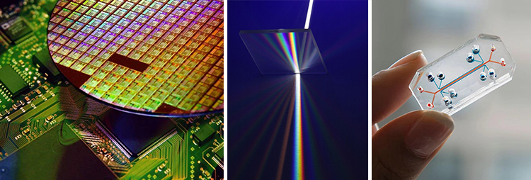
In semiconductor chip manufacturing, optical component processing, and biomedical device research and development fields, the processing accuracy of micro-nano structures is constantly advancing towards atomic-level. Due to the constraint of the wavelength diffraction limit, traditional lithography technology not only faces the problem of a sharp increase in cost when the processing scale enters below 10nm, but also the bottleneck of a significant increase in process complexity. Nanoimprint technology is gradually becoming one of the core technologies in the next-generation micro-nano manufacturing field with its significant advantages in high-resolution processing, low-cost production and high mass production efficiency.
(Note: Image from online resources)
Ⅰ
Nanoimprint: The "Movable Type Printing" in Chip Manufacturing Field
1、Background: An Inevitable Choice to Break through the "Ceiling" of Lithography
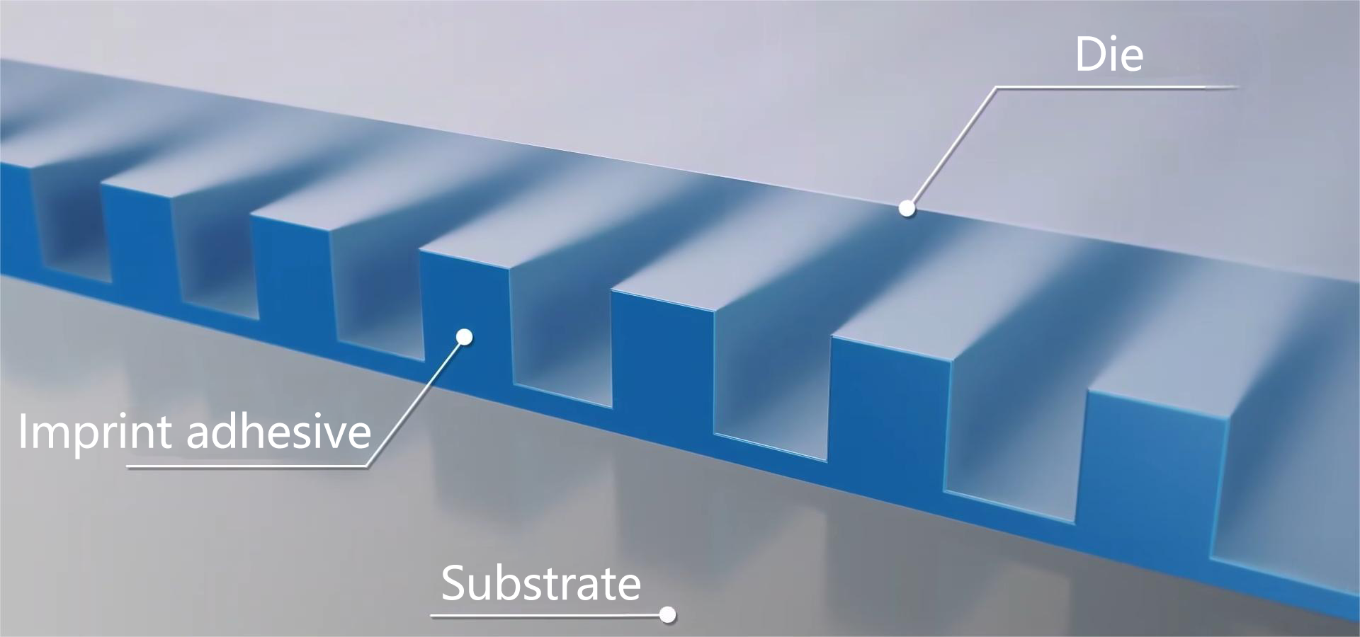
Nanoimprint Lithography (NIL) is a new and breakthrough micro-nano processing technology. It replicates the micro-nano structure patterns on the die onto the substrate coated with polymer materials through physical imprinting. Its core idea is similar to the ancient seal printing technique, but it achieves high-precision pattern replication at the nanoscale.
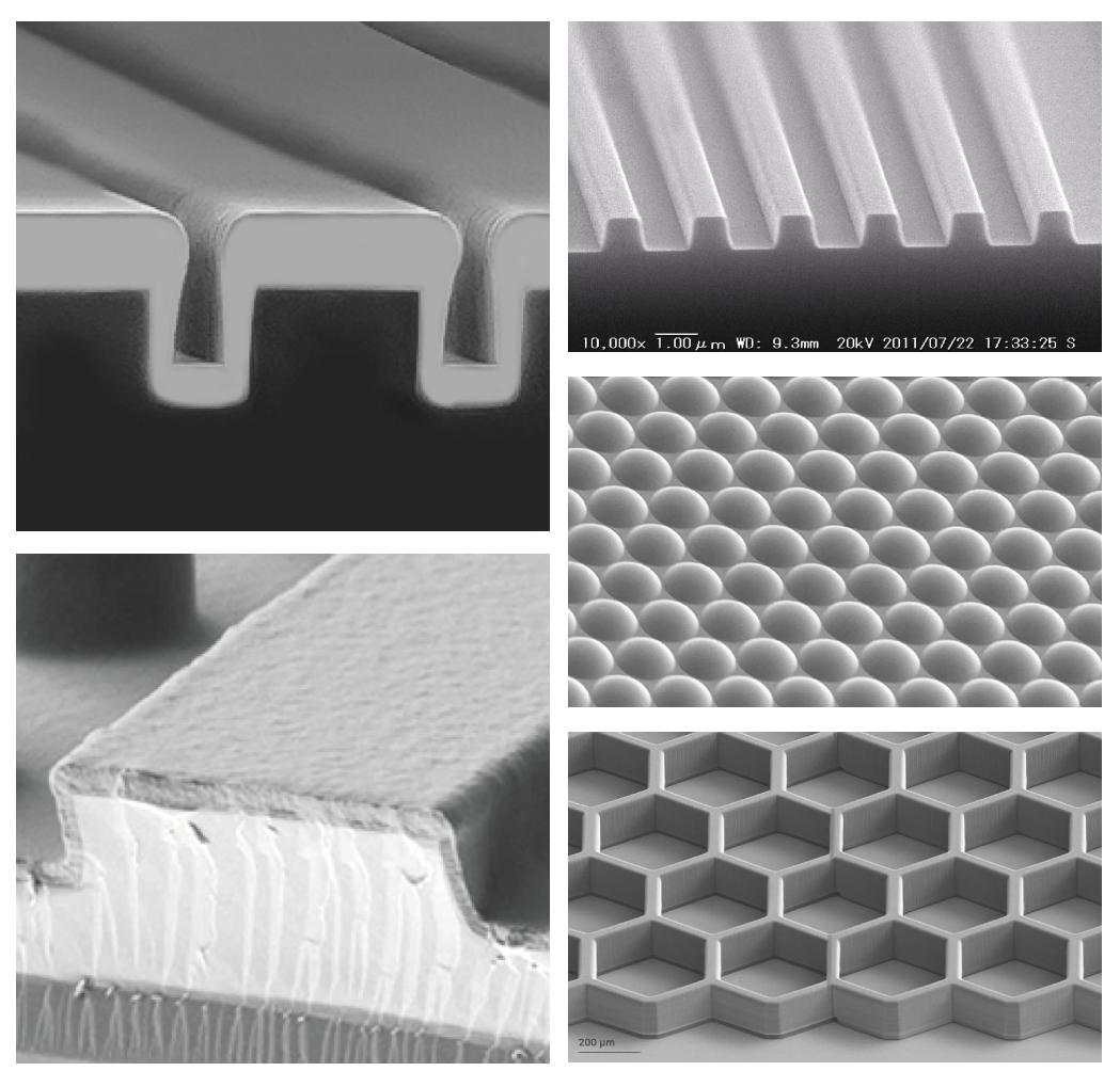
In the 1990s, the semiconductor industry accelerated the miniaturization process of chip manufacturing. Traditional optical lithography technology was limited by the diffraction limit of light, and the minimum feature size was difficult to break through the resolution limit. Although electron beam lithography could achieve a precision of less than 100 nanometers, its scanning processing efficiency was extremely low, and the equipment and process costs were high, which could not meet the requirements of large-scale mass production. At this critical juncture in technological development, nanoimprint technology emerged. Its core advantage is: by using die replication instead of beam scanning, nanoscale patterns can be imprinted onto the substrate in one go. This not only significantly reduces production costs but also achieves a resolution of less than 5nm.
2、 Technical Principle: Nanoscale "Stamping Art"
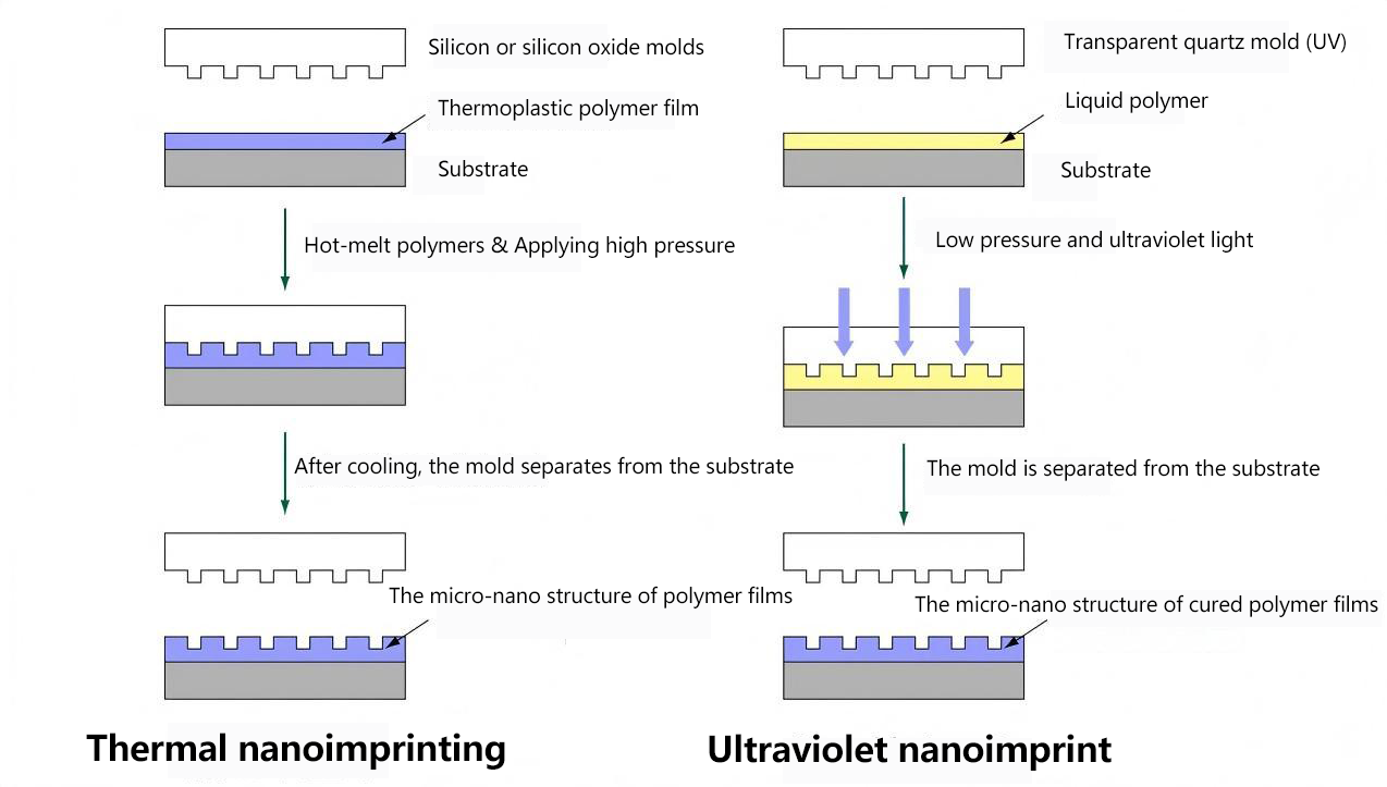
The essence of nanoimprint is graphic replication: By using a die with nanoscale patterns, precise pressure is applied to a substrate coated with photoresist to shape the photoresist layer according to the die's contour. After curing, the die is peeled off, leaving a complementary nanostructure on the substrate. According to different curing methods, it is mainly divided into types such as thermal nanoimprint (heating and softening the adhesive layer), UV nanoimprint (UV light curing the adhesive layer), and micro-contact printing (soft etching). The core process of nanoimprinting includes key links such as die preparation, imprinting adhesive coating, imprinting forming, demolding and post-treatment.
Ⅱ
Key Process Breakdown: The "Precision Game" Layer by Layer
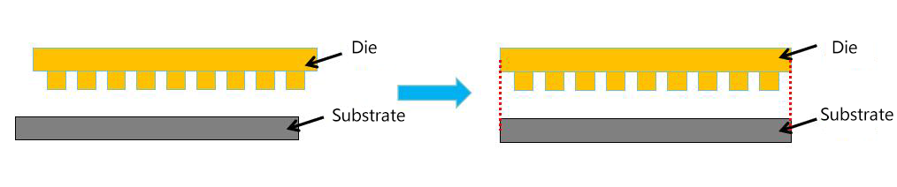
1. Die Preparation - Nanoscale Alignment
First of all, a die with the required nano-pattern (commonly known as a "seal" or "mold") should be made. The die material needs to be hard and durable (such as silicon or quartz, etc.), and its surface pattern is processed through high-precision techniques such as electron beam lithography or focused ion beam etching. Before using the prepared die for imprinting, the die and the substrate need to be aligned at the sub-nanometer level. Traditional mechanical positioning systems are limited by mechanical gaps and thermal drift, which may be difficult to meet the requirements.
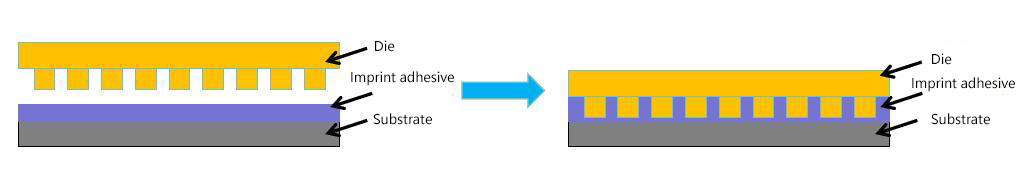
2.Impression Forming - Pressure Uniformity Control
The production of nanoimprint technology uses physical contact for graphic transfer. The die is pressed into the imprint adhesive (polymer layer) under certain pressure to fill the concave structures on the die. This can achieve a very high resolution, with the minimum resolution being less than 5 nanometers. For instance, in hot embossing, the contact pressure between the die and the base needs to be evenly distributed; otherwise, it may lead to uneven thickness of the adhesive layer, and the pattern may appear uneven.
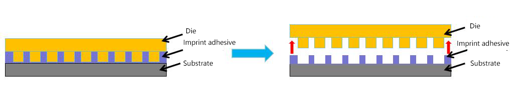
3.Demolding - Stress Control
After the polymer gets solid, carefully separate the die from the substrate. At this point, a nanostructure pattern complementary to the template is formed on the polymer layer. During demolding, the adhesion force between the template and the solid adhesive layer can easily cause the nanostructure to tear, which requires precise control. For example, the demolding speed and displacement accuracy can be dynamically adjusted at the micrometer level.
Ⅲ
The Pain Point of Converting Piezoelectric Technology into Nanoimprint
The piezo nano-positioning stage (such as the X, Y, θz 3-axis system) is driven by piezoelectric ceramics, with a linear resolution of up to 2nm. Under closed-loop control, the positioning accuracy is ≤10nm. Combined with real-time feedback from sensors, it can achieve sub-micron coarse alignment and nano-level fine alignment between the die and the substrate before impression, ensuring the overlap between pattern layers.
The piezoelectric ceramic actuator array can achieve multi-point independent pressure control. By adjusting the pressure at each point in real time through a closed-loop feedback system, the uniformity of pressure can be maximized. Technical advantages: The piezo drive has a fast response speed and can dynamically compensate for the pressure attenuation caused by temperature changes during the embossing process, avoiding the "hysteresis effect" of traditional mechanical pressurization.
The piezo nanopositioning stage, when equipped with a force sensor, can achieve low-speed demolding control, monitor the demolding force changes and adjust the displacement speed in real time to reduce stress concentration.
CoreMorrow Piezo Nanopositioning System
The "Precise Hand" of Nanoimprint
The evolution of nanoimprint technology is essentially a philosophy of balancing precision requirements and cost control. The piezo nano-positioning and control system is precisely the core element in this philosophical practice - from alignment to imprinting, from curing to demolding, behind every nano-scale action, there is a need for ultimate control accuracy as support.
(The motion of piezo nano-positioning stage)
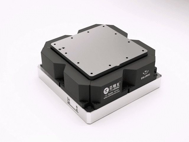
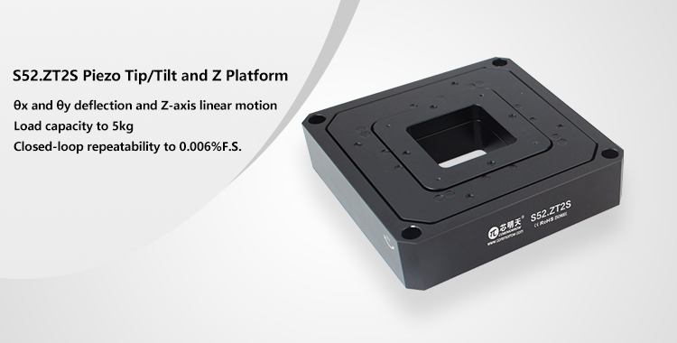
S52 Large Load Piezo Tip/Tilt and Z Platform
S52.ZT2S piezo tip/tilt and Z platform can generate θx and θy deflection as well as linear motion in Z direction. It has a load capacity of 5kg, and the closed-loop repeatability positioning accuracy of 0.006%F.S., which is suitable for various high-precision application fields. Meanwhile, it has a 55×55mm ² through hole at the center, which is suitable for transmitted light applications.
Characteristics
|
Model |
|
|
|
|
|
|
|
|
Nominal travel in Z(0~120V) |
|
|
Max.travel in Z(0~150V) |
|
|
Nominal travel in θx, θy(0~120V) |
±1.10mrad/axis(≈±227”) |
|
Max.travel in θx, θy(0~150V) |
±1.37mrad/axis(≈±282.5”) |
|
Sensor |
|
|
Closed-loop resolution in Z |
|
|
Closed-loop resolution in θx, θy |
0.14μrad(≈0.03”) |
|
Closed-loop linearity in Z |
|
|
Closed-loop linearity in θx, θy |
|
|
Closed-loop repeatability in Z |
|
|
Closed-loop repeatability in θx, θy |
|
|
Blocking force in Z |
|
|
Stiffness in Z |
|
|
El. capacitance |
|
|
Load capacity |
|
|
Unloaded resonant frequency |
|
|
Resonant frequency@2.5kg |
|
|
Step Time@2.5kg |
|
|
Pitch angle in Z |
|
|
Yaw angle in Z |
|
|
Roll angle in Z |
|
|
Coupling in X/Y |
|
|
Coupling in horizontal direction |
|
|
Mass(Cable included) |
|
|
Material |
Steel/Aluminum |
H30 Piezo Scanning and Rotation Stage
H30 is a piezo scanning and rotation stage with 3 axes motion in X, Y and θz, and with a Ø60mm central large aperture. It adopts frictionless flexible hinge structure design, featuring fast response speed and high precision of closed-loop positioning. The central large aperture makes it easy to integrate into microscopic and scanning optical system.

Characteristics
|
Model |
|
|
Active axes |
|
|
Drive control |
4 driving channels ,3 sensing channels |
|
Linear travel range(0~120V) |
±56μm/axis |
|
Max.linear travel range(0~150V) |
±70μm/axis |
|
Tilt angle(0~120V) |
1.6mrad(≈330”) |
|
Tilt angle(0~150V) |
2mrad(≈413”) |
|
Sensor |
|
|
Resolution in XY |
|
|
Resolution in θz |
0.3μrad(≈0.06”) |
|
Linearity in XY |
|
|
Linearity in θz |
|
|
Repeatability in XY |
|
|
Repeatability in θz |
|
|
Unloaded resonant frequency |
|
|
Loaded resonant frequency@6kg |
|
|
El. capacitance |
|
|
Step time |
|
|
Load capacity |
|
|
Material |
Aluminum alloy |
|
Mass |
|
Sweep, get the latest information on core tomorrow
Address:1F, Building I2, No.191 Xuefu Road, Nangang District, Harbin, China
Tel:0451-86268790
Piezo · Nano · Motion
